
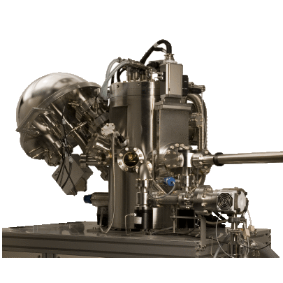
X-Ray Photoelectron Spectroscopy (XPS) – also known as Electron Spectroscopy for Chemical Analysis (ESCA) – is a very suitable method to analyse the chemical composition of any surface. Be it either solid or in powdered form with XPS we can investigate very different materials. Even residuals from liquid solutions can be analysed, once filtered and dried. With an information depth of not more than 10 nm XPS is a very surface sensitive method. In combination with layer by layer material removal through argon ion etching it is also possible to derive depth profile until depths of 1-2 μm. Thanks to imaging-XPS (i-XPS) we can, not only identify differences in the elemental distribution, but also display and analyse these with chemical mapping.
Photoelectron spectroscopy is based on the photoelectric effect. On the surface electrons are emitted from atoms by intensive stimulation with X-rays. The energy of the emitted electrons is measured with a special detector and from this, the binding energy of the electrons is computed. Since elements and compounds have typical binding energy, it is now possible to characterize the analyzed surface both in a qualitative and a quantitative way.
The location of the emitted electrons is determined by rastering of a focussed X-ray over the surface. Like this, the spectra can be traced back to every point on the area so that XPS measurements can be distinctly quicker and easier analyzed and understood thank to i-XPS. Thus it is possible to generate an exact map of all elements on a certain surface area, e.g. of a stain or contamination.
As we are able to scale down the diameter of the X-ray beam at our XPS system to 10 μm, even single features with only a few μm size can be analysed. On the other side of the scale we are able to scan areas as large as 1400 x 1400 μm.
Benefits of this analyzing technique
- Qualitative and quantitative analysis of the surface composition
- Identification of binding and oxidation states, as well as chemical functional groups
- Verification of all elements except H and He
- Thickness measurements of surface coatings from 1 to 10 nm
- Compilation of depth profiles (10 nm ot 2 μm)
- Development of stacking-/layermodels
- Possibility of 2-dimensional imaging of the chemical distribution of elements
Materials and Dimensions
- Solid material (e.g. metal, ceramic or plastic)
- Conductive and isolating substrates
- Cross-section dimension: 95 mm / height: max. 10 mm
- Powder, textile and structured surfaces
Contact us – and fathom new aspects of the properties of your product!